2025-05-27
PCBA factory role in Electronic Product Design
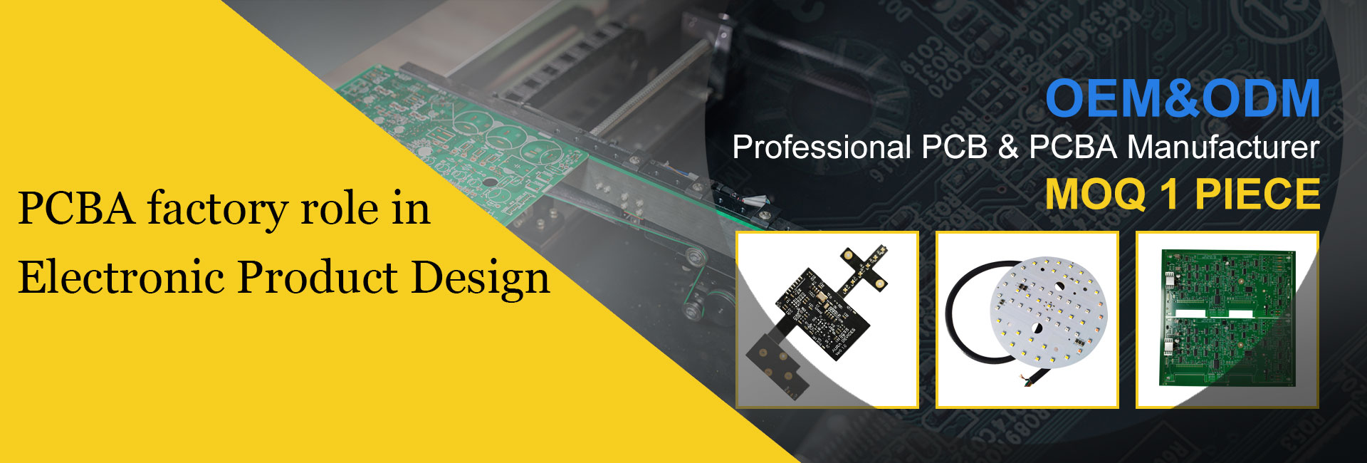
The core role of PCBA factory
PCBA factories assume key technical support and production conversion responsibilities in the field of electronic product research and development and design, and their role covers the entire life cycle from proof of concept to mass production. The following is a structured analysis of its core role:
Design optimization and verification support
PCB layout and signal integrity optimization
PCBA factories use professional design tools (such as Cadence, Altium) to help optimize circuit board layout to ensure the integrity of high-speed signals and high-frequency circuits (such as RF communication modules). For example, multilayer PCB designs follow strict impedance control and electromagnetic compatibility (EMC) guidelines, and factory engineers can provide layout advice to reduce interference.
Proof and prototype verification
Verify the feasibility of the design by rapid proofing (such as 24-hour prototype production), and find potential problems (such as solder joint reliability, thermal management), thereby shortening the iteration cycle. For example, the KLS PCB factory provides rapid prototyping services for multi-layer PCBs and high-frequency boards that can support early design verification.
Technical integration of production processes
SMT and DIP process adaptation
PCBA factories select appropriate patch (SMT) or plug-in (DIP) processes based on component types (such as BGA, 0201 components) to optimize production efficiency. For example, KLS Circuit supports high-density component assembly, ensuring the mounting accuracy of 0201/01005 components.
Materials and process selection
Recommend substrates (such as FR4, aluminum substrates, high-frequency Rogers materials) and surface treatment processes (HASL, ENIG) according to product requirements. For example, medical equipment requires lead-free processes, while high-frequency communication modules require low-loss materials.
Cost and supply chain management
BOM optimization and procurement support
Factory assists in optimizing bill of materials (BOM) and reducing costs through bulk procurement. For example, KLSPCB provides component purchasing services and integrates supply chain resources.
Mass production cost control
Reduce production costs through process optimization (such as reducing the number of layers and simplifying the lamination process). For example, the blind buried hole design of HDI boards can reduce interlayer connection costs.
Quality and reliability guarantee
Full process quality control
AOI optical detection, X-RAY detection, flying needle testing and other technologies are used to ensure the yield rate. For example, KLS Circuit's SMT production line is equipped with AOI equipment, which can achieve 100% defect screening.
Environmental adaptability verification
Provide high-temperature aging tests, vibration tests, etc. to ensure that the products meet the reliability requirements of industrial control, automotive electronics and other scenarios.
Customization and innovation support
Special process development
Provide solutions for customized needs (such as flexible PCBs, metal core PCBs). For example, KLSPCB supports rigid-flex bonding boards (Rigid-Flex) and aluminum-based heat sinks.
Quickly respond to the market
Support agile development through small batch trial production (such as 24-hour fast proofing) to accelerate product launch.
Summarize
The PCBA factory is not only the executor of production, but also the partner of design optimization. Its core value lies in reducing R&D risks, shortening cycles and enhancing product competitiveness through technology integration, process innovation and quality control. If you need to know more about specific cases and project needs, you can contact us and get a faster quote.
PCBA factory role in Electronic Product Design What is SMT and PCBA? What is different between PCB and PCBA?