What is SMT and PCBA?
Surface-Mount Technology and Printed Circuit Board Assembly: Foundations of Modern Electronics Manufacturing
Executive Summary
Modern electronics, from compact consumer devices to complex industrial and medical systems, are fundamentally reliant on sophisticated manufacturing techniques that enable miniaturization, enhanced performance, and cost-effective mass production. At the core of this capability are Surface-Mount Technology (SMT) and Printed Circuit Board Assembly (PCBA). SMT is a precise method for mounting electrical components directly onto the surface of a printed circuit board, revolutionizing component density and automated assembly. PCBA, in turn, represents the comprehensive process that transforms a bare circuit board into a fully functional electronic system through the meticulous integration of components, primarily utilizing SMT. This report delves into the definitions, processes, benefits, and widespread applications of SMT and PCBA, highlighting their synergistic relationship as indispensable elements that drive continuous innovation and shape the technological landscape.
Introduction: The Foundation of Modern Electronics
The pervasive presence of electronic devices in contemporary society, spanning from ubiquitous smartphones and smart home gadgets to highly specialized industrial control systems, advanced medical equipment, and critical aerospace components, underscores the profound impact of modern manufacturing techniques. These techniques are not merely incremental improvements but are crucial enablers for achieving the unprecedented levels of miniaturization, heightened performance, and cost-effective mass production that define today's technological advancements. Without these sophisticated processes, the intricate and compact electronic systems that power our world would be impractical, if not impossible, to produce.
Within this critical domain, Surface-Mount Technology (SMT) and Printed Circuit Board Assembly (PCBA) stand as foundational processes. They represent the pivotal stages that bridge the gap between raw electronic components and bare circuit boards, transforming them into intelligent, functional electronic systems. The continuous evolution and refinement of SMT and PCBA have been instrumental in propelling the current technological revolution, facilitating the creation of increasingly complex, compact, and powerful electronic products that are integrated into nearly every facet of daily life and industrial operation. These technologies are not just manufacturing steps; they are the bedrock upon which the vast majority of modern electronic innovation is built.
Surface-Mount Technology (SMT): Revolutionizing Component Placement
Surface-Mount Technology (SMT) represents a pivotal advancement in electronics manufacturing, defining a method where electrical components, specifically known as Surface-Mount Devices (SMDs), are mounted directly onto the surface of a Printed Circuit Board (PCB). This approach fundamentally diverges from older methodologies, such as Through-Hole Technology (THT), which required component leads to be inserted through pre-drilled holes in the PCB.
Originally termed "planar mounting," SMT's conceptualization dates back to the 1960s, with IBM pioneering its initial application in the construction of small-scale computers. Despite its early development, SMT's widespread adoption and emergence as the dominant assembly method gained substantial momentum around 1986, largely due to its inherent advantages in efficiency, component density, and suitability for automation compared to its predecessors.
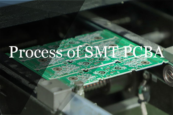
The SMT Manufacturing Process: A Step-by-Step Guide
The SMT process is characterized by its multi-step, highly automated nature, meticulously engineered for unparalleled precision and manufacturing efficiency.
- Solder Paste Application: This critical initial step involves the precise deposition of solder paste onto designated pads on the PCB surface. Solder paste is a meticulously formulated mixture comprising microscopic solder alloy particles combined with flux. The application is executed using a solder paste printer, which employs a stencil—also referred to as a solder screen or template—to ensure that the paste is accurately applied only to the specific areas where components will be mounted. This process is analogous to screen-printing, but with solder paste instead of ink. Ensuring the correct quantity of paste on each pad is imperative for establishing reliable electrical connections.
- Component Placement: Following the application of solder paste, highly advanced automated "pick-and-place" machines precisely position the SMDs onto their respective solder pads on the PCB. These sophisticated machines retrieve components from various feeders, such as reels, tubes, and waffle trays, and are capable of placing an astonishing volume of components, up to 80,000 individual components per hour, demonstrating exceptional speed and accuracy. Precision at this stage is paramount, as even a minor misalignment can compromise the board's functionality.
- Reflow Soldering: Once all components are accurately placed, the populated PCB is conveyed through a reflow oven. Within the oven, the board is subjected to a carefully controlled temperature profile that heats the solder paste to its melting point. As the solder liquefies, it forms robust electrical and physical connections between the component leads and the PCB pads. Precise temperature management is critical to prevent thermal damage to sensitive components or the formation of improper solder joints. A notable characteristic of molten solder is its surface tension, which inherently pulls components into alignment with their solder pads, effectively correcting minor placement inaccuracies and improving assembly yield.
- Inspection and Quality Control: Throughout the SMT manufacturing process, and particularly after reflow soldering, multiple rigorous inspection points are integrated to ensure the highest quality standards are met. This comprehensive inspection includes visual checks, Automated Optical Inspection (AOI) machines to detect defects such as misplaced components, poor solder joints, or missing parts, and for more complex or multi-layered boards, X-ray inspection to examine hidden connections like Ball Grid Arrays (BGAs). Post-soldering cleaning processes may also be employed to remove any residual flux or contaminants that could affect the board's long-term performance and reliability.
The SMT process is a cornerstone of modern electronics manufacturing, characterized by its precision and efficiency. The following table outlines the key steps involved:
Step Number |
Step Name |
Brief Description of Action |
Purpose/Outcome of Step |
Key Equipment Used |
| 1 | Solder Paste Application |
Precise deposition of solder paste onto designated PCB pads using a stencil. |
Prepares the board to hold and bond components; ensures accurate solder volume. |
Solder Paste Printer, Stencil (Solder Screen/Template) |
| 2 | Component Placement |
Automated machines precisely position Surface-Mount Devices (SMDs) onto solder-pasted pads. |
Populates the PCB with electronic components in their correct locations. |
Pick-and-Place Machines |
| 3 | Reflow Soldering |
Populated PCB passes through an oven, melting solder paste to form connections. |
Creates strong electrical and physical connections between components and the board. |
Reflow Oven |
| 4 | Inspection & Quality Control |
Boards undergo visual, optical, and X-ray inspections; cleaning may occur. |
Detects defects (misplaced components, bad solder joints, contaminants); ensures quality. |
AOI Machines, X-ray Inspection, Visual Inspection Tools, Cleaning Systems |
Core SMT Components and Essential Equipment
The highly automated SMT process relies on specifically designed electronic components and a suite of specialized machinery.
SMT Components (SMDs): These electronic components are engineered for surface mounting, distinguished by their compact size and lighter weight compared to traditional through-hole components. They encompass a wide array of device types:
- Passive Components: This category includes resistors, typically rectangular in shape to optimize board space, and capacitors, which are often flat and available in various package styles, along with inductors.
- Two-terminal devices: Examples include diodes.
- Three-terminal devices: Such as Small Outline Transistors (SOTs).
- Integrated Circuits (ICs): Encompassing a broad range of packages including SOIC, SSOP, TSSOP, SOJ, QFP, PGA, and BGA. Specialized packages like DPAK (TO-252) are frequently used for medium to high-power transistors and diodes, designed for efficient heat dissipation while maintaining a compact footprint. Chip-on-Board (COB) technology involves directly mounting and connecting a bare semiconductor die to the PCB, further maximizing space efficiency and achieving ultra-low-profile designs.
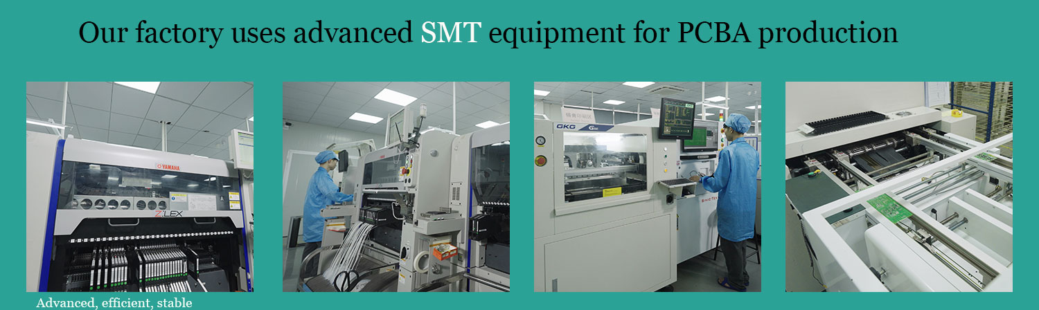
Essential SMT Equipment: The highly automated SMT process relies on a suite of specialized machinery:
- Solder Paste Printer: A precision machine responsible for applying solder paste onto the PCB through a stencil.
- Pick-and-Place Machines: Automated robotic systems that accurately pick up and place SMDs onto the solder-pasted PCB.
- Reflow Oven: An electronic heating apparatus that melts the solder paste, creating permanent electrical and mechanical connections between components and the board.
- Inspection Equipment: Includes Automated Optical Inspection (AOI) systems, X-ray inspection machines, and manual visual inspection stations to detect defects and ensure quality.
- Ancillary Equipment: A range of supporting machinery such as solder paste mixers, PCB racks, PCB support systems, cleaning systems (for flux residue removal), nitrogen generators (for inert reflow atmospheres), and automated storage systems for components.
Advantages and Disadvantages of SMT
SMT has profoundly impacted electronics manufacturing, offering numerous advantages, but also presenting certain limitations.
Advantages: