
Introduction And Related Knowledge About Gold-Plated Circuit Boards
Gold-Plated Circuit Boards (Gold-Plated Circuit Boards) are circuit boards that have a layer of gold plated on the surface of the PCB, a treatment that improves the board's electrical conductivity, abrasion resistance, and oxidation resistance. Here is some key information about Gold-Plated Circuit Boards and what they do:
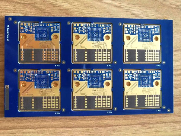
1. Role of gold plating:
- Gold plating effectively prevents PCB oxidation and corrosion, increasing the reliability and life of the board.
- Gold is highly conductive and corrosion resistant, enabling the creation of reliable solder joints.
- Gold plating is dense and relatively wear-resistant, and is typically used for soldering and plugging applications.
2. Types of Gold Plating:
- Electroplated Gold (Electroplated Gold): A layer of gold is deposited on the surface of the PCB through an electrolytic process, providing excellent electrical conductivity and corrosion resistance, and is commonly used in high-reliability applications such as aerospace and military.
- Chemical Gold (Immersion Gold): does not depend on the current, through a chemical reaction on the PCB surface to form a thin layer of gold, often used as a protective layer to prevent oxidation of the copper layer.
- Soft Gold (Soft Gold): Gold alloy with a higher proportion of pure gold, softer and more flexible, suitable for applications that require repeated plugging and unplugging, such as connectors.
- Hard Gold: Gold alloys doped with other metals such as nickel or cobalt are harder and more wear-resistant, suitable for applications requiring high wear resistance and reliability.
3. Gold Plating Process:
- Includes surface preparation (cleaning to remove oil and oxidized layers), copper plating to improve electrical connectivity, gold plating (electroplating or chemical gold) and post-treatment (rinsing and drying).
4. Advantages of gold plating:
- Improved corrosion resistance, the gold layer prevents corrosion of the PCB by environmental factors.
- Enhanced wear resistance and reduced contact resistance, especially in applications requiring frequent contact.
- Stress control and ease of bonding processing, immersion gold-plated boards are easier to control the stress and are suitable for bonding processing.
- Extended storage life, the pending life of gold-plated plates is many times longer than that of lead-tin alloys.
- Improved signal transmission, especially in high-frequency signal transmission applications, immersed gold-plated boards are better able to maintain signal integrity.
5. Applications for gold-plated circuit boards:
- Gold-plated circuit boards are widely used in applications requiring long-term storage, high reliability and high-frequency applications, such as telecommunications, aerospace and medical technology.
With the above information, we can see that gold plated circuit boards play an important role in the modern electronics industry due to their excellent electrical conductivity, abrasion resistance and oxidation resistance.
Gold-Plated PCB Boards: An In-Depth Exploration
Gold-plated PCB boards are a specialized type of printed circuit board that offer several distinct advantages. These boards are created by electroplating a layer of hard gold on the surface of PCB circuit board pads. The process involves dissolving nickel and gold in a chemical solution, immersing the circuit board in an electroplating cylinder, and applying an electric current to generate a nickel-gold coating on the copper foil.
The Role of Gold Plating
-
Gold plating serves two primary functions: wear resistance and corrosion resistance. Parts with sockets and gold fingers, as well as areas in contact with conductive rubber, need to be gold plated. Circuit boards operating in highly corrosive environments also benefit from gold plating as it prevents oxidation and protects the underlying nickel and copper layers. Gold is wear-resistant and provides good reliability.
-
Gold-plated PCB boards offer strong conductivity, excellent oxidation resistance, and a long service life. The coating is dense and relatively wear-resistant, making it ideal for welding and socket applications. The gold plating process is widely used in circuit board components such as solder pads, gold fingers, connector shrapnel, and other positions. The most commonly used handheld circuit boards are often gold-plated.
-
Gold plating has low contact resistance, good conductivity, easy welding, strong corrosion resistance, and certain wear resistance (in the case of hard gold). As a result, it is widely used in precision instruments, printed circuit boards, integrated circuits, tube shells, electrical contacts, and other fields.
The Difference between Soft Gold and Hard Gold
In the PCB gold plating process, hard gold plating is also known as an electroplating alloy. It has been alloyed with other elements to increase its hardness, while soft gold plating is pure gold. Hard gold plating is suitable for areas such as gold fingers and keyboards that require friction. Soft gold is commonly used for aluminum or gold wiring on COB (on board chips).
The Difference between PCB Gold Deposition and Plating
- Process Principle: PCB gold deposition is a process of depositing metal ions on the surface of a circuit board. The circuit board is immersed in a solution containing gold salts and reducing agents, and gold ions are reduced to metal and deposited on the surface of the circuit board. Gold plating, on the other hand, involves immersing a circuit board in a solution containing gold salts and applying electricity to deposit gold ions on the surface of the circuit board.
- Metal Thickness: The metal thickness of PCB sinking gold and plating gold is different. Gold deposition can form a relatively thick metal layer, typically reaching 2-5 microns. The gold plated metal layer is relatively thin, usually only around 0.5-1.5 microns.
- Metal Color: The metal colors of PCB sinking gold and gilding are also different. The metal color of heavy gold is golden yellow, while the metal color of gilding is light yellow.
- Surface Flatness: The surface flatness of PCB sinking gold and gold plating is also different. The surface of the sinking gold is relatively flat, ensuring high-quality welding and contract performance. The surface of gold plated is relatively rough, which can lead to welding and contact problems.
- Cost: The cost of PCB gold deposition and plating is also different. The cost of sinking gold is relatively high due to the need for more chemical reagents and a longer processing time. The cost of gold plating is relatively low because of its shorter processing time and simpler operation.
Process Flow of PCB Gold Plating
Gold-plated PCB boards are widely used in precision instruments, printed circuit boards, integrated circuits, tube shells, electrical contacts, and other fields due to their low contact resistance, good conductivity, easy welding, strong corrosion resistance, and certain wear resistance. The process flow of PCB gold plating includes:
-
Surface treatment: Clean the surface of the PCB to remove oil stains, burrs, oxide layers, etc.
-
Electroplating: Place the PCB into the electroplating bath and add the plating solution. The electroplating solution contains a reducing agent that can reduce the gold atoms on the PCB surface into metal ions and deposit them on the PCB surface.
-
Water washing: After electroplating, a layer of metal deposition forms on the surface of the PCB, which needs to be cleaned with water.
-
Drying: Place the PCB in a drying oven and dry with water.
-
Adhesive application: Apply a layer of conductive adhesive to the surface of the PCB to ensure good contact between the PCB and other devices.
-
Recycling: Remove the PCB from the adhesive tape and place it in the recycling bin.
The gold-plated PCB board can play a protective role. The gold-plated layer can protect the circuit board from oxidation, corrosion, and other effects, increasing the service life of the circuit board. Additionally, metals themselves have good conductivity, which can improve the conductivity of PCBs and reduce line impedance.
How to choose Gold-Plated Circuit Boards
When selecting a gold-plated circuit board, several factors need to be considered to ensure that the quality and performance of the board meets the needs of the specific application. The following are some key factors and recommendations:
1. Material selection:
- Select a high-quality base material, such as FR4, to ensure the durability, conductivity and performance of the gold fingers. Gold plating should be 99.7% or higher purity gold for better conductivity and corrosion resistance.
2. Thickness of gold plating:
- Determine the thickness of the gold plating based on the application requirements. Common thicknesses range from 1 to 5 microinches (25 to 127 microns) for electroless nickel immersion gold (ENIG) to 10 to 50 microinches (0.25 to 1.27 microns) for electroplated gold. For connectors and contacts, the recommended gold thickness is 0.76
to 1.27 microns (30 to 50 microinches).
3. Design Considerations:
- The thickness of the gold plating and the quality of the metal substrate need to be considered in the design. The gold plating thickness should not be less than 30 microinches to ensure durability and conductivity. Also, consider the chamfer angle of the gold finger, which should typically be set between 30 and 45 degrees for ease of insertion and removal.
4. Manufacturing Best Practices:
- Manufacturing gold finger PCBs requires complex steps, including first creating a PCB layout and then fabricating the actual printed circuit board using appropriate materials such as FR4.
5. Surface Preparation:
- Ensure that the substrate surface is clean and in optimal condition for optimal gold layer adhesion.
6. Gold Plating Method Selection:
- Select electroless or electroplated based on cost, thickness requirements and substrate characteristics.
7. Industry Standards:
- Follow industry standards, such as IPC-4552, to ensure quality and consistency of gold plated PCBs.
8. Performance requirements:
- Select the appropriate gold plating method based on performance requirements. For example, ENIG (electroless nickel immersion gold) is commonly used in consumer electronics, while electroless gold plating is often used in high-reliability applications such as aerospace and military.
9. Cost versus long-term value:
- While the initial cost of gold plating may be high, it saves money in the long run by reducing maintenance, failures and extending product life.
10. Design constraints:
- Consider gold plating specifications such as layer thickness and substrate material compatibility, which may introduce design constraints.
11. Material compatibility:
- Ensure that the selected material is compatible with the gold plating to avoid adhesion problems and long-term reliability issues.
12. Manufacturing Process:
- The gold plating process is complex and requires precise control of chemistry and timing.
By taking all of these factors into consideration, a gold-plated board can be selected for a specific application, ensuring high performance and long-term reliability of the product.
(0Products)
Data is empty