
Multilayer Pcb Board Design |Kinglisheng Factory
Customized Double Layer Pcb One-stop Service
The multilayer PCB board is a revolutionary component in the world of electronics. Comprised of multiple layers of conductive materials and insulating substrates, it offers exceptional electrical performance and reliability.
These boards are designed to handle complex circuitry, enabling the integration of numerous electronic components. With advanced manufacturing techniques, multilayer PCB boards ensure precise signal transmission and reduced interference.
They find applications in a wide range of industries, from consumer electronics to aerospace and telecommunications. The durability and compactness of multilayer PCB boards make them an ideal choice for modern, space-saving designs.
Choose multilayer PCB boards for superior quality and performance in your electronic projects. |Multilayer PCB |Electronics Components |pcba AdvancedTechnology.
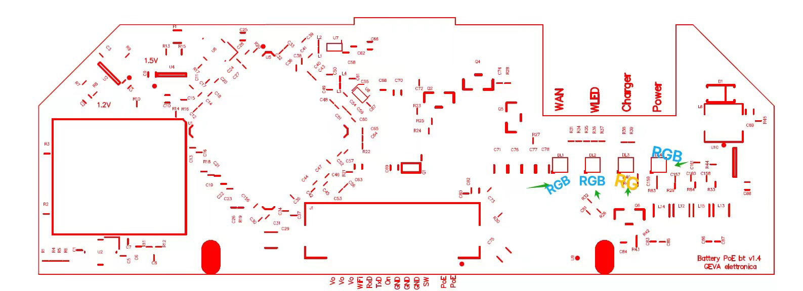
Multilayer printed circuit boards (PCBs) offer numerous advantages over single or double-layered PCBs. Here are the advantages of using multilayer PCBs:
1. Increased Component Density: Multilayer PCBs use thin substrate layers between copper traces, which enables designers to incorporate more components in a smaller space. This allows for more functionality to be packed into smaller devices and can take advantage of advancements in miniaturization technology.
2. Improved Signal Integrity: In multilayer PCBs, multiple layers of power and ground planes or signal layers help to reduce electromagnetic interference (EMI) and electromagnetic radiation (EMR). This allows for better signal quality and integrity, which can improve circuit performance and minimize the risk of signal degradation.
3. Enhanced Thermal Management: Multilayer PCBs with power or ground planes help to dissipate heat more efficiently. This makes them ideal for high-temperature applications that require reliable and efficient heat dissipation.
4. Reliability: Multilayer PCBs are less prone to failure compared to single-layer or double-layered PCBs. The additional internal planes help to strengthen the board's structure, reduce the risk of signal line interference, and increase the board's overall reliability.
5. High-Speed Performance: Multilayer PCBs have a shorter signal path, allowing for quicker signal transmission. This makes multilayer PCBs ideal for high-speed applications, including telecommunications, data transfer, and high-speed computing applications.
Overall, multilayer PCBs offer a wide range of advantages compared to single or double-layered PCBs. They provide improved functionality, signal integrity, thermal management, and reliability, making them an ideal choice in a wide range of applications.
1. Increased Component Density: Multilayer PCBs use thin substrate layers between copper traces, which enables designers to incorporate more components in a smaller space. This allows for more functionality to be packed into smaller devices and can take advantage of advancements in miniaturization technology.
2. Improved Signal Integrity: In multilayer PCBs, multiple layers of power and ground planes or signal layers help to reduce electromagnetic interference (EMI) and electromagnetic radiation (EMR). This allows for better signal quality and integrity, which can improve circuit performance and minimize the risk of signal degradation.
3. Enhanced Thermal Management: Multilayer PCBs with power or ground planes help to dissipate heat more efficiently. This makes them ideal for high-temperature applications that require reliable and efficient heat dissipation.
4. Reliability: Multilayer PCBs are less prone to failure compared to single-layer or double-layered PCBs. The additional internal planes help to strengthen the board's structure, reduce the risk of signal line interference, and increase the board's overall reliability.
5. High-Speed Performance: Multilayer PCBs have a shorter signal path, allowing for quicker signal transmission. This makes multilayer PCBs ideal for high-speed applications, including telecommunications, data transfer, and high-speed computing applications.
Overall, multilayer PCBs offer a wide range of advantages compared to single or double-layered PCBs. They provide improved functionality, signal integrity, thermal management, and reliability, making them an ideal choice in a wide range of applications.
Multilayer Pcb Board Design What to Consider
When designing multilayer PCB boards, the following key factors need to be considered to ensure board performance, reliability and manufacturability:
1. Component layout and routing:
- Careful component layout is critical to optimize signal integrity, thermal management, and space optimization. Critical components such as microcontrollers and power supplies should be prioritized, followed by passive components such as resistors and capacitors. Layout should consider power and ground plane placement, decoupling capacitors, and proper wiring techniques to minimize noise and interference.
2. Layer Structures and Routing Strategies:
- Layer structure and routing strategy are key considerations in PCB design. Deciding on the number of layers, their arrangement and routing strategy affects signal integrity, EMC and manufacturability. Multi-layer PCBs provide greater routing flexibility and allow for better power and ground plane distribution. Proper layer stack planning considers impedance control, signal integrity and separation of sensitive circuits to optimize device performance.
3. Power and ground plane design:
- Power and ground plane design is critical to minimize noise, achieve proper signal return paths, and ensure efficient power distribution. A robust ground plane and well-designed power distribution network help minimize voltage drops, maintain signal integrity, and prevent electromagnetic interference. Properly placed decoupling capacitors and carefully routed power supply alignments enhance power integrity and stability, especially for high-speed and mixed-signal designs.
4. Design for Testability (DFT):
- Design for Testability considerations make it possible to efficiently test and troubleshoot PCBs during production and maintenance. Hardware designers need to incorporate test points, such as test pads and vias, to facilitate electrical testing and inspection.DFT techniques also include design for circuit testing (ICT), boundary-scan testing (JTAG), and built-in self-test (BIST) capabilities for enhanced test coverage and fault detection.
5. Design Rule Check (DRC) and Design for Manufacturability (DFM):
- Design Rule Checking (DRC) and Design for Manufacturability (DFM) are important components of PCB design.DRC ensures that the design follows manufacturing rules and constraints, minimizing the risk of errors, shorts, and other manufacturing issues.DFM considerations focus on optimizing the design for efficient manufacturing processes such as boarding, solder paste mask and silk screen alignment, component placement, and proper pads for cost-effective and high quality manufacturing.
6. Electromagnetic compatibility (EMC) and safety:
- EMC should be considered during design to ensure that the equipment operates in its intended electromagnetic environment and does not generate or suffer electromagnetic interference. Safety is a key consideration for any electronic device and PCB design should consider isolation and insulation techniques to prevent electrical shock and improve safety.
7. Thermal management:
- Thermal management of multilayer PCBs is critical to reliability and performance. Key techniques include the use of heat vias/heat pads attached to the internal planar layers, the use of copper planes as heat spreaders, increasing the thickness of copper in the external layers, applying solder paste masks (SMOBCs) to bare copper, and providing adequate airflow paths around the components.
8. Signal Integrity:
- Maintaining signal integrity in multilayer boards is more challenging because of increased crosstalk and coupling between parallel layers. Strategies include assigning continuous reference planes to signals, using low-loss dielectric materials, controlling trace impedance through all layer transitions, applying ground protection traces around sensitive signals, incorporating shielded ground planes between critical networks, and providing proper decoupling and termination for power distribution.
9. Cost considerations:
- As multilayer PCB complexity increases, so does manufacturing cost. Key cost factors include number of layers, board size, higher densities, advanced materials, and low yields.
10. Reliability Considerations:
- The reliability of multilayer PCBs is affected by manufacturing process controls, laminate material quality, and design factors such as internal layer thermal dissipation, mechanical reinforcement and stiffness, component layout, and density.
By taking these factors into account, multilayer PCBs can be designed for superior performance, manufacturability, and reliability.
How to Choose the Right Multilayer Pcb Board
The following key factors need to be considered when choosing the right multilayer PCB board:
1. Project complexity:
- For high complexity projects that require a large number of components and complex wiring, multilayer PCBs are ideal as they offer a more compact layout to save space.
2. Space constraints:
- If the project has stringent size requirements, multilayer PCBs can achieve a more compact design by utilizing Z-axis space.
3. Signal Integrity Requirements:
- High-speed or high-frequency applications require signal integrity and mutual isolation to be considered, and multilayer PCBs can provide better control impedance and reduced crosstalk.
4. Power requirements:
- For applications requiring high current or high power, the inner layers of a multilayer PCB can be used to distribute power and ground and help manage heat dispersion.
5. Cost Budget:
- Multilayer PCBs cost more than single or double layer boards, so budget is also an important consideration in the selection process.
6. Thermal Management:
- The inner planes of a multilayer board can help dissipate heat if the project generates more heat.
7. Frequency and speed:
- For radio frequency (RF) applications or high-speed digital circuits, a multilayer layout provides better control of characteristic impedance and reduces interference between signals.
8. Number of Layers Determination:
- The process of determining the number of PCB layers should take into account factors such as the number of signal networks, device density, PIN density, frequency of signals and board size.
9. Material Selection:
- Selection of the appropriate PCB material, the main concern is the dielectric constant Er and material tangent tan δ. The higher the dielectric constant, the stronger the ability of the electromagnetic field to conduct in the material. And the larger the material tangent tanδ, the greater the signal loss.
10. impedance control:
- From the consideration of signal integrity, it is required to realize the matching of impedance on the signal transmission path. Generally take the single-ended signal to ground impedance of 50Ω, while the differential pair of inter-signal impedance is 100Ω.
11. EMC performance:
- In the design of the laminated structure, it is also necessary to consider the requirements of the EMC performance, through a reasonable laminated structure design to improve the EMC performance of the PCB.
12. Board thickness selection:
- Board thickness selection for multilayer PCBs is a critical design decision that directly affects circuit performance, reliability, and cost-effectiveness. Thinner PCBs help reduce signal loss and crosstalk, thereby improving signal integrity.
13. Thermal management capability:
- The board thickness of a multilayer PCB also affects its thermal management capabilities. A thicker PCB provides more space for a large ground plane or power plane, which helps to disperse heat and improve thermal efficiency.
By taking all of these factors into consideration, you can choose the most appropriate type of multilayer PCB for your project. Remember to work with an experienced PCB supplier during the decision-making process to ensure the performance and reliability of the final product.
(0Products)
Data is empty