
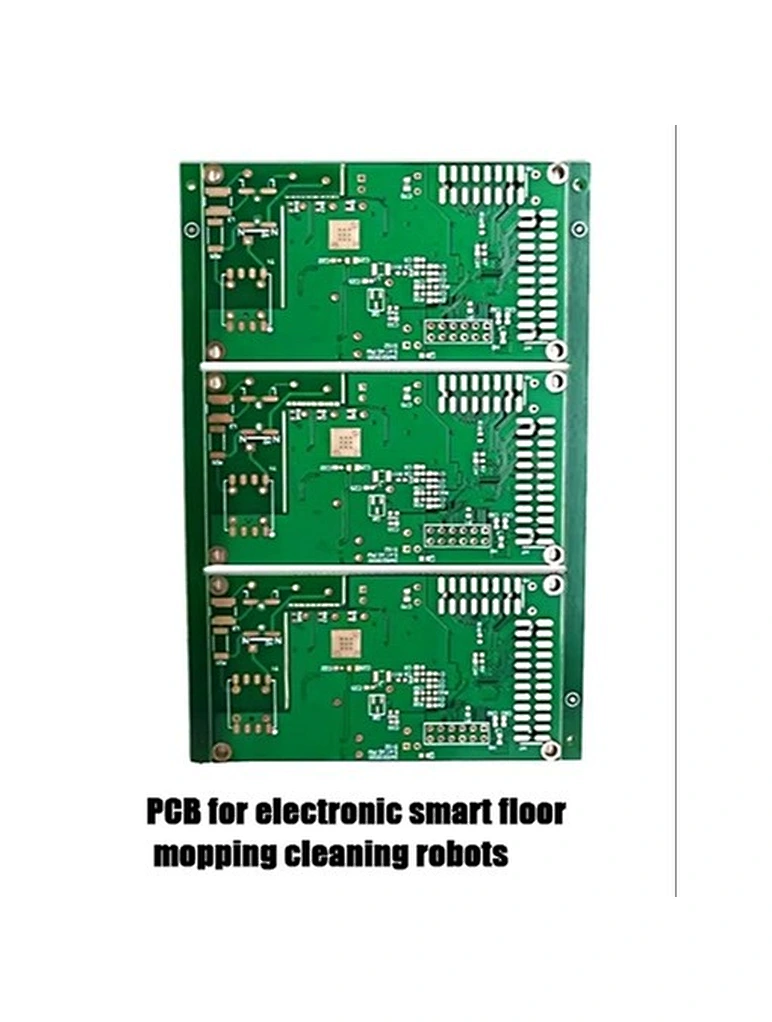
Manufacturing and assembly of PCB for electronic smart floor mopping cleaning robots
Product Description
Basic Info.
Model NO. | SMS-001 | Layers | Multilayer |
Base Material | FR-4 | Certification | RoHS, CCC, ISO |
Customized | Customized | Condition | New |
Material | Fr4, Aluminum, Pi | Color | Green, Blue, White, Red, Yellow, Black |
| Thickness | 0.2mm-6mm | Copper Thickness | 0.5oz-5oz |
Transport Package | Vacuum Package | Trademark | OEM/ODM |
Origin | Shenzhen,China | HS Code | 85340090 |
Packaging & Delivery
Package Size | customized |
Package Gross Weight | 0.300kg |
| Delicery Time | 7-20days |
Company Information
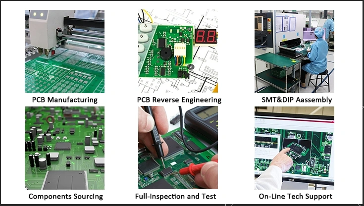
• Multi-layer Circuit Board Manufacturing (1-32L)
• Global Component Procurement & BOM Optimization
• SMT Assembly with 01005 Package Capability
• Box Build Assembly & Functional Testing
• Rapid Prototyping (24hr Quick-turn PCB)
• Compliance Certification Support (CE/FCC/RoHS)
Our advantage
Precision-Centric Quality Assurance System
Compliant with IPC-6012B Class 3 aerospace-grade PCB specifications and IPC-600G Class acceptability standards, our manufacturing processes hold dual certifications:
ISO 9001:2015 Quality Management System (QMS)
UL 94V-0 Flame-Retardant Material Certification
Multi-Stage Verification Protocols:
Pre-Production Validation
Flying Probe Testing (≤0.1Ω impedance tolerance)
Signal Integrity Simulation (HyperLynx®)
In-Line Quality Control
X-Ray Inspection (0.15mm microvia detection)
3D AOI (Omron VT-M121) with 15μm resolution
Functional Compliance
ICT Testing (Keysight 3070 platform)
MIL-STD-202G Environmental Stress Screening
Sustainable Electronics Manufacturing
ROHS 3 (EU 2015/863) & REACH SVHC compliance
Halogen-Free PCB Materials (IEC 61249-2-21)
Conflict Minerals (Dodd-Frank 1502) Sourcing Policy
We have a lot of R&D experience and technical advantages in various PCB products.
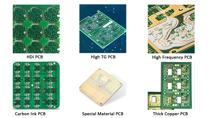
| HDI PCB | HDI PCB boards utilize blind vias and buried vias technology, incorporating precision microvias with diameters ≤0.006". This advanced interconnect architecture delivers 60%+ higher circuitry density compared to traditional FR-4 circuit boards, enabling compact multilayer designs for high-frequency applications. |
| High TG PCB | General TG plate is over 130 degrees, high TG is generally above 170 degrees, and medium general TG between 150–130. |
| High Frequency PCB | RO4003C, RO4350B, Ro3003,Ro3010,and RT5880 etc operating frequency around 500MHz to 2GHz, they are used in powerdevider,radar,satellite system, mobile phone receive base station and so on. |
| Carbon Ink PCB | Very high resitance value carbon ink pcb will well supply goodconductivity, was often been applied in automotive filed,medicalelectronics,communication equipment etc..; . |
| Special Material PCB | Rogers4003,Rogers4550,Arion 25FR, 25N for Ceramic PcB filling.Atlion series, Taconic series,Arlon series,Nelco series etc. PTFE highfrequency material. |
| Thick Copper PCB | Ensure there is enough thick plating in the hole to guarantee resistance fall inside allowed range of process requirement 70% circuitboard to finish use of 35um copper foil thickness, there are some ones use 70um105um at most140um nut less copper thickness and cycle on. |
PCB Technical Specification
| Order Quantity | 1-500,000 |
| Layer | 1.2.4,6,up to 32 layer |
| Material | FR-4,glass epoxy,FR4 High Tg,Rohs compliant,Aluminum,Rogers,etc |
| PCB type | Rigid,flexible,rigid-flexible |
| Shape | Any shape:Rectangular,round,slots,cutouts,complex,irregular |
| Max PCB dimensions | 20 inch*20 inch or 500mm*500mm |
| Thickness | 0.2~4.0mm,Flex 0.01-0.25" |
| Thickness tolerance | +10%/-10% |
| Copper thickness | 0.5-4oz |
| Copper thickness tolerance | +0.25oz/-0.25oz |
| Surface finish | HASL,Nickle,lmm Gold,lmm Tin,lmm Silver,OSP etc |
| Solder mask | Green, red,white,yellow,blue,black, Double-sided |
| Silk screen | White,yellow,black,or negative, Double-sided or single-sided |
| Silk screen min linewidth | 0.006"or 0.15mm |
| Min drill hole diameter | 0.01.0.25mm.or 10 mil |
| Min trace/gap | 0.075mm or 3mil |
| PCB cutting | Shear,V-score,tab-routed |
PCBA Capabilities
| Turnkey PCBA | PCB+components sourcing+assembly+package |
| Assembly details | SMT and Thru-hole.lSO SMT and DlP lines |
| Lead Time | Prototype:7 work days. Mass order: 7-20 work days |
| Testing on products | Flying Probe Test, X-ray Inspection, AOl Test, Functional test |
| Quantity | Min quantity:1pcs.Prototype, small order, mass order, all OK |
| Files needed | PCB: Gerber files(CAM, PCB, PCB DOC) |
| Components: Bill of Materials(BOM list) | |
| Assembly: Pick-N-Place file | |
| PCB Panel Size | Min size: 0.25*0 25 inches(6*6mm) |
| Max size: 20*20 inches(500*500mm) | |
| PCB Solder Type | Water Soluble Solder Paste, RoHS lead free |
| Components details | Passive Down to 0201 size |
| BGA and VFBGA | |
| Leadless Chip Carriers/CSP | |
| Double-sided SMT Assembly | |
| Fine Pitch to 0 .8mils | |
| BGA Repair and Reball | |
| Part Removal and Replacement | |
| Component package | Cut Tape,Tube,Reels,Loose Parts |
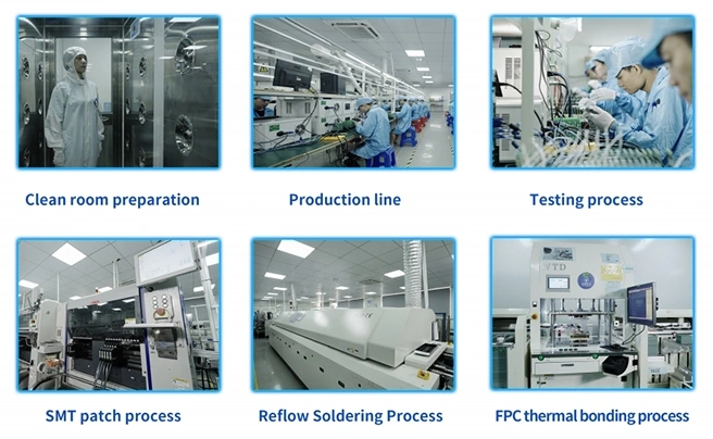
| PCB assembly process | drilling-----exposere----plating----etaching&stripping----punching----electrical testing----smt----wave----soldering----assembling----ict----functing testing----temperature&humidity testing |
PCB Production Line
Some of the products we serve:
- Flex PCB
- Rigid Flex PCB
- Gold Panel
- HDl Board
- Tin Panel
- Gold Finger PCB
- Heavy Copper PCBs
- PCB Assembly
Lead Time
| PCB | ||
| Layer | Quick Turn/Usual Time | Mass production |
| 2L | 24hours/ 4-5days | 8-10days |
| 4L | 48hours/6-7days | 10-12days |
| 6L | 72hours/7-8days | 12-14days |
| 8L | 72hours/8-10days | 16-18days |
| 10L | 96hours/12-14days | 18-20days |
| .................. | ........... | ........... |
| Assembly | ||
| Quantity | Usual time | |
| <20pcs | 2days | |
| 20-100pcs | 3days | |
| 100-1000pcs | 6days | |
| >1000pcs | depend on bom |
FAQ
- Q: What do I need to provide to get a PCB and PCBA quotation?A: Gerber file, PCB technical specifications, quantity, and BOM list.
- Q: Will you check my files before production? A: Yes, our engineers will check your Gerber file and BOM list to avoid any mistakes.
- Q: What kind of PCB file format do you accept for production? What CAM software do you use? A: We accept Gerber files for production. We use CAM350, GENESIS, and UCAM GC-CAMMV-2000 software.
- Q: Can you design Gerber files? A: Yes, we can design Gerber files if the customer provides a schematic. Schematic samples can also be provided if the customer wants one.
- Q: For turnkey assembly orders, what is your component procurement process? A: If we don't have the components in stock, we order them in bulk according to your Bill of Materials (BOM) to ensure cost savings. For hard-to-find or rarely used parts, we typically add 5% as spares. We contact the customer for approval on order minimums.
- Q: What is the minimum order size for turnkey assembly orders? A: We don't have a minimum order size. However, larger orders can result in greater cost savings.
- Q: What is the lead time for PCBA? A: 8-10 days for samples, and 15-20 days for bulk orders.
- Q: How about delivery? A: It depends on the customer. We sometimes ship through our forwarder, who has better rates with DHL, TNT, UPS, FedEx, etc. If the customer has their own express account, we can also arrange shipment based on that.
- Q: My budget is limited, can you provide solutions to save costs? A: Yes, we can. For example, we can replace DIP components with SMD components to reduce the PCB size, re-layout the PCB to reduce its size, or recommend alternative components.

