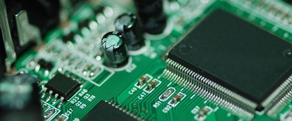
Design requirements of PCB board for SMT process

In the process of SMT patch processing, all processing equipment has the characteristics of full automation, precision and speed. Then PCB design must meet the requirements of SMT chip processing equipment to effectively ensure product quality.
1. PCB shape design
The PCB shape design is generally rectangular, and the aspect ratio is 4:3 or 3:2. The area of the board surface is not easy to be too large during the design of the board, so as to avoid deformation in the high temperature state of reflow soldering, which affects the quality of the original component and the overall appearance. The area of the PCB should be combined with the thickness. The thinner the PCB, the smaller the PCB should be within a reasonable range.
2. PCB size design
When designing a PCB, it is necessary to consider the maximum size and minimum size of the SMT chip processing equipment. At present, the installation scope of different types of SMT processing equipment in the SMT industry is similar. (Minimum size=50mm*50mm, Maximum size=510mm*460mm) When the PCB design size is smaller than the equipment required minimum size of 50mm*50mm, then the way of imposition should be considered. And the imposition method must meet the requirements of SMT equipment, and V-shaped grooves or stamp holes are used between the panels. Ensure that the imposition of the processing process can be effectively divided.
3. PCB thickness design
The design of PCB board thickness mainly considers the body strength and high temperature reflow soldering deformation during SMT chip processing. It should be determined according to the external dimensions, the number of layers, the quality of the installed components, the chip processing method and the impedance. Generally, the allowable PCB thickness of the transmission track of SMT chip processing equipment is between 0.5mm and 5mm.
4. PCB process side design
In the SMT patch production process, the PCB is completed by the track transmission of the processing equipment. In order to ensure that the PCB is reliably fixed, the processing process requirements should be considered before the PCB board design, and the size of the reserved process side (long side) is 3mm -5mm, which can effectively ensure the fixed work of the equipment. SMD components are not allowed within the range required by the process side. When the space cannot be reserved, the process side must be added.
5. PCB component layout design
1). When the mounted PCBA is in the reflow soldering process, PCB design should consider the solder-ability of the device. Ensure that the long sides of the component pins should be perpendicular to the transmission direction of the reflow soldering, so as to ensure that the device pins are heated and soldered at the same time, and avoid tombstones and empty soldering problems in the soldering process.
2). The design and arrangement of the components on the PCB board are uniform, high-power, large-volume, and distributed to avoid local heat absorption stress during the reflow soldering process, resulting in non-wetting between the components and the pad and forming an empty solder False welding affects the reliability of the circuit.
3). Large-scale components with panel-mounted IC, PLCC, QFP, BGA, and high-height components cannot be placed on the wave soldering surface of the plug-in. It will affect the height of the spray tin to not reach the solder joints during wave soldering, resulting in undesirable phenomena such as empty soldering and short-circuiting.
The above is design requirements of PCB board for SMT process, have you learned it?