2025-05-12
what is double layer pcb?
what is double layer pcb?
A double-layer printed circuit board (also known as dual-layer printed circuit board) is a printed circuit board that consists of two conductive layers separated by an insulating dielectric material. Below are some of the main aspects of a double-layer printed circuit board:
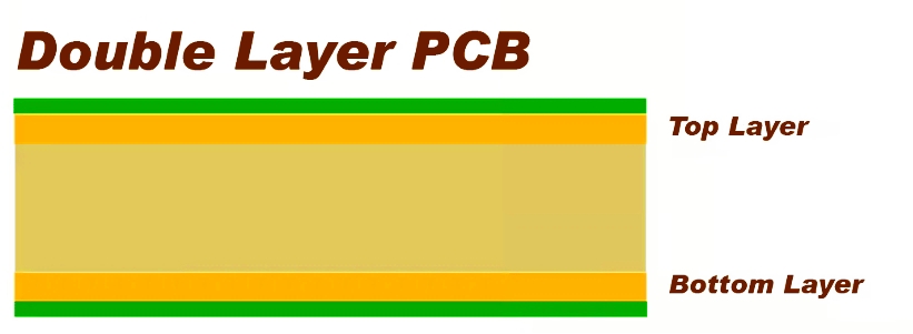
Basic Structure
- Two conductive layers: These layers are usually made of copper and can be found on the top and bottom sides of the board. They provide the necessary electrical connections for the components.
- Dielectric: This material, usually a fiberglass-reinforced epoxy laminate (FR4), is sandwiched between the two conductive layers to prevent electrical short circuits and provide structural support.
Design and Manufacturing
- Design Flexibility: Dual layer boards offer more design options than single layer boards. Designers can route wires on both sides, allowing for more complex circuits.
- Manufacturing Process: The manufacturing process includes etching, drilling and plating. Through-holes are used to create electrical connections between two layers of circuit boards.
Applications.
- Consumer Electronics: Used in devices such as smartphones, tablets and laptops where space is limited and complex circuitry is required.
- Industrial: Motor controllers, power supplies and automation systems where reliability and performance are critical.
Advantages
- Space efficiency: Compact design utilizing both sides of the board.
- Improved Signal Integrity: Ability to decentralize circuits and reduce interference between signals.
Disadvantages
- Increased complexity: More complex design and manufacturing processes than single-layer printed circuit boards.
- Higher Cost**: Typically more expensive than single-layer PCBs due to increased materials and manufacturing steps.
Future Trends
- Material Advances: Development of new materials to improve performance.
- Miniaturization: The constant push for smaller, more efficient designs.
Dual-layer printed circuit boards are a fundamental technology in modern electronics, striking a balance between complexity and functionality for a wide range of applications. As technology evolves, we can expect further innovations in the design and manufacture of double-layer printed circuit boards.